

Hey there! As a supplier of Hybrid Dielectric PCBs, I'm super stoked to share with you the different inspection methods for these awesome boards. Hybrid Dielectric PCBs are pretty unique because they combine different dielectric materials, which allows for better performance in various applications. So, let's dive right into how we can make sure these PCBs are up to snuff.
Visual Inspection
First off, one of the most basic yet crucial inspection methods is visual inspection. This is like the first line of defense. You just take a good look at the PCB to spot any obvious issues. You're checking for things like scratches, cracks, or any signs of damage on the surface. Sometimes, there could be misaligned components or soldering defects that are visible to the naked eye.
When you're doing a visual inspection, it's a good idea to use a magnifying glass or a microscope. This helps you see the tiny details that might be missed otherwise. For example, you can check the soldering joints to make sure they're smooth and there are no cold solder joints. Cold solder joints can cause intermittent connections, which is a big no - no in PCB performance.
X - Ray Inspection
X - ray inspection is another powerful tool in our inspection arsenal. It's especially useful for checking the internal structure of the Hybrid Dielectric PCB. Since these PCBs can have multiple layers, it's hard to know what's going on inside just by looking at the surface. X - ray inspection allows us to see through the layers and check for things like proper alignment of vias, which are the small holes that connect different layers of the PCB.
If a via is misaligned, it can cause electrical shorts or impedance issues. X - ray inspection can also detect any hidden voids in the solder joints. These voids can weaken the connection and lead to reliability problems down the line. It's like having a super - power to see what's hidden beneath the surface.
Automated Optical Inspection (AOI)
Automated Optical Inspection, or AOI for short, is a high - tech way to inspect PCBs. It uses cameras and advanced software to scan the PCB and compare it to a pre - defined standard. AOI can quickly detect a wide range of defects, such as missing components, wrong component placement, and soldering issues.
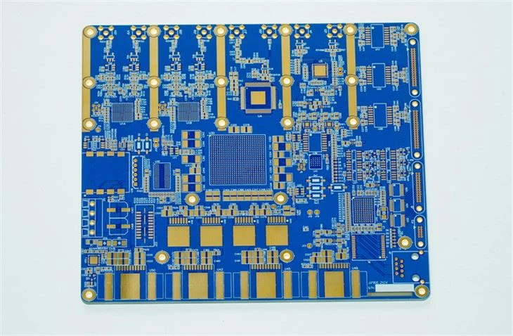

The great thing about AOI is that it's really fast. It can inspect a large number of PCBs in a short amount of time, which is super important for mass production. And it's also very accurate. The software can detect even the tiniest defects that might be difficult for a human to spot.
In - Circuit Testing (ICT)
In - Circuit Testing is all about testing the electrical performance of the PCB. It involves connecting the PCB to a test fixture and applying electrical signals to different points on the board. This allows us to check if the components are working properly and if there are any electrical shorts or opens.
For Hybrid Dielectric PCBs, ICT is crucial because these boards are often used in high - performance applications where electrical reliability is key. By testing the electrical performance, we can make sure that the PCB will function as expected in its intended application.
Flying Probe Testing
Flying Probe Testing is a flexible and efficient way to test PCBs. Instead of using a fixed test fixture like in ICT, flying probe testers use movable probes to make contact with the test points on the PCB. This makes it a great option for testing small - batch or prototype PCBs.
Flying Probe Testing can quickly test a wide range of electrical parameters, such as resistance, capacitance, and continuity. It's also very useful for detecting shorts and opens in the PCB. And because it doesn't require a custom test fixture, it can save a lot of time and money, especially for smaller production runs.
Thermal Imaging
Thermal imaging is a method that can help us identify hot spots on the PCB. When a PCB is in operation, different components generate heat. If there are any issues with the components or the design, it can cause abnormal heat distribution.
By using a thermal imaging camera, we can see where the hot spots are on the PCB. This can help us identify potential problems, such as overheating components or poor heat dissipation. For Hybrid Dielectric PCBs, which are often used in high - power applications, thermal imaging is an important tool to ensure the long - term reliability of the board.
Impedance Testing
Impedance testing is crucial for Hybrid Dielectric PCBs, especially those used in Microwave High Frequency PCB and Low Noise High Frequency PCB applications. Impedance is the measure of the opposition to the flow of alternating current in a circuit.
If the impedance of the PCB is not within the specified range, it can cause signal reflections, which can degrade the performance of the circuit. Impedance testing involves using specialized equipment to measure the impedance at different points on the PCB. This helps us ensure that the PCB meets the electrical requirements of the application.
Material Analysis
Since Hybrid Dielectric PCBs are made up of different dielectric materials, it's important to do material analysis. This can help us make sure that the right materials are used and that they have the correct properties.
Material analysis can involve techniques such as spectroscopy and microscopy. These techniques can help us identify the chemical composition and structure of the dielectric materials. By doing material analysis, we can ensure that the Hybrid Dielectric PCB has the desired electrical and mechanical properties.
Surface Finish Inspection
The surface finish of a PCB is important for both its appearance and its performance. A good surface finish can protect the PCB from corrosion and improve the solderability of the components.
We can use various methods to inspect the surface finish, such as visual inspection and chemical analysis. Visual inspection can help us spot any visible defects, such as uneven plating or scratches. Chemical analysis can help us determine the composition and thickness of the surface finish.
Coating Inspection
Many Hybrid Dielectric PCBs are coated with a protective layer to enhance their performance and durability. Coating inspection is important to make sure that the coating is applied evenly and that it has the right properties.
We can use methods like visual inspection and adhesion testing to inspect the coating. Visual inspection can help us see if there are any bubbles or cracks in the coating. Adhesion testing can determine how well the coating is bonded to the PCB surface.
Conclusion
As you can see, there are many different inspection methods for Hybrid Dielectric PCBs. Each method has its own advantages and is used to check different aspects of the PCB. By using a combination of these methods, we can ensure that our High - Precision Hybrid Dielectric PCB meet the highest quality standards.
If you're in the market for Hybrid Dielectric PCBs, whether it's for Antenna Circuit Board or Flexible High Frequency PCB applications, we'd love to have a chat with you. We can discuss your specific requirements and how our inspection methods can ensure that you get the best - quality PCBs for your needs. Reach out to us and let's start a conversation about your PCB procurement.
References
- "PCB Design and Manufacturing Handbook"
- "High - Frequency PCB Design: Theory and Applications"
- "Advanced PCB Testing Techniques"